
The Cause of PCB Bening and Warping Issue
May 10 , 2021The Cause of PCB Bening and Warping Issue
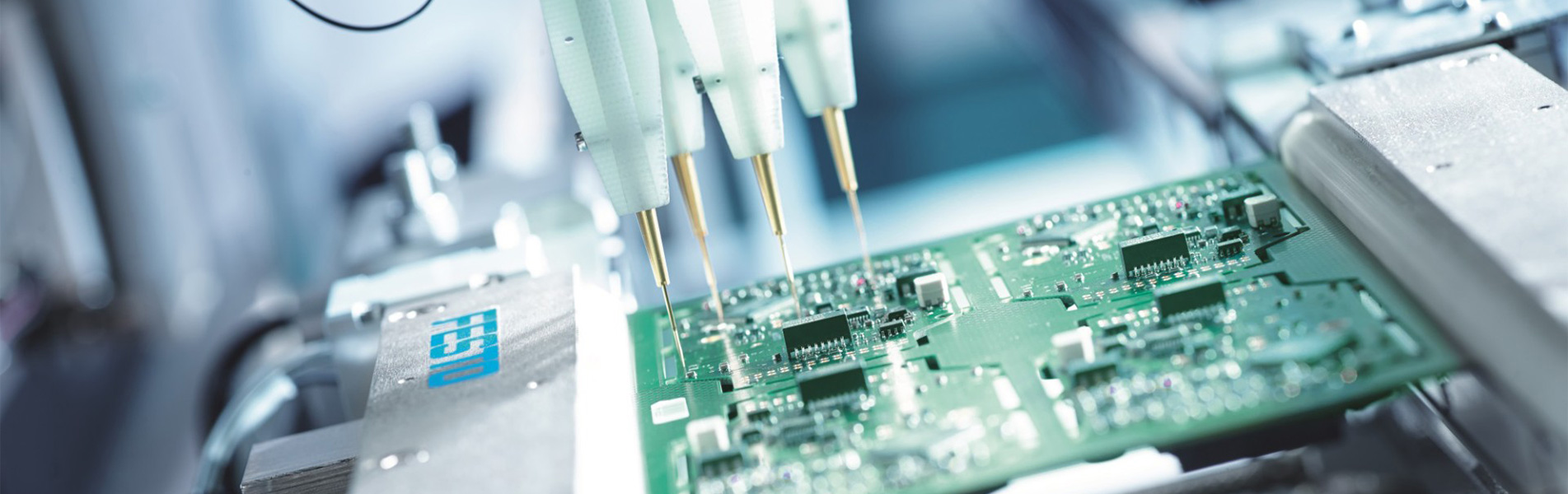
In the SMT process, most of the circuit boards are prone to board bending and warping when passing through Reflow. In severe cases, it may even cause components such as empty soldering and tombstones. How can we overcome it?
The cause of each board bending and board warping may be different, but it should all be attributed to the stress applied to the board being greater than the stress that the board material can withstand. When the board is subjected to uneven stress or When the ability of each place on the board to resist stress is uneven, the result of board bending and board warping will occur.
Where does the stress on the board come from? In fact, the biggest source of stress in the Reflow process is "temperature". Temperature not only makes the circuit board soft, but also distorts the circuit board. In addition, the material characteristics of "thermal expansion and contraction" are the main cause of bending and warping of the board.
1. The uneven copper surface area on the circuit board will worsen the bending and warping of the board.
Generally, a large area of copper foil is designed on the circuit board for grounding purposes. Sometimes a large area of copper foil is also designed on the Vcc layer. When these large area copper foils cannot be evenly distributed on the same circuit board At this time, it will cause the problem of uneven heat absorption and heat dissipation. Of course, the circuit board will also expand and contract with heat. If the expansion and contraction cannot be performed at the same time, it will cause different stress and deformation. At this time, if the temperature of the board has reached Tg The upper limit of the value, the board will begin to soften, causing permanent deformation.
2. The connection points (vias) of each layer on the circuit board will limit the expansion and contraction of the board
Today's circuit boards are mostly multi-layer boards, and there will be rivet-like connection points (via) between the layers. The connection points are divided into through holes, blind holes and buried holes. Where there are connection points, the board will be restricted. The effect of expansion and contraction will also indirectly cause plate bending and plate warping.
3. The weight of the circuit board itself will cause the board to dent and deform.
Generally, the reflow furnace uses a chain to drive the circuit board forward in the reflow furnace, that is, the two sides of the board are used as fulcrums to support the entire board. If there are heavy parts on the board, or the size of the board is too large, It will show a depression in the middle due to the amount of seed, causing the plate to bend.
4. The depth of the V-Cut and the connecting strips will affect the deformation of the jigsaw.
Basically, V-Cut is the culprit that destroys the structure of the board, because V-Cut cuts V-shaped grooves on the original large sheet, so the V-Cut is prone to deformation.
Huizhou Fusen Intelligent Technology Co., Ltd.


 English


 IPv6 network supported