
Hot-bar process details
Sep 24 , 2022Hot-bar process details
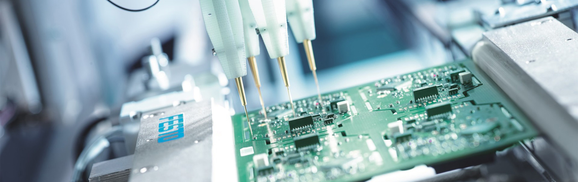
1. Hot-bar process principle
Hot-bar process is a common name for heating and melting tin welding. In short, this process is to heat two parts coated with flux and tin to a temperature sufficient to melt the solder (melting point of lead-free solder: 217 ℃). After cooling and curing, the two parts form a permanent electrical and mechanical connection through the cured solder.
2. Hot-bar process application
For devices that cannot be welded by SMT + reflow furnace, we can use constant temperature soldering iron for manual welding. However, manual welding has defects such as inconsistent and uneven operation of operators, and even faulty welding or damaged products. The pulse hot press is different from the constant temperature soldering iron. The pulse hot press can reach the required temperature at the moment of power on. Once the voltage is not applied at both ends of the indenter, the air cooling can quickly reach the room temperature and the indenter is flat. Therefore, the welded products have consistent appearance, stable yield and simple operation.
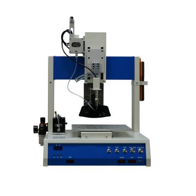
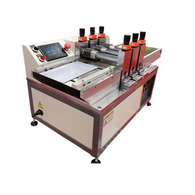
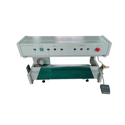
3. Hot-bar process example

4. Hot-bar tin quantity
control
1.
Selection of pin center distance (pitch) and gold finger gap: generally, the
pin center distance (pitch) of two materials used in the soldering process
should be greater than or equal to 1.0mm, because the large spacing can ensure
that the products are not easy to be short circuited due to the solder balls.
If the product space is insufficient, the pitch can also be less than 1.0mm,
but not less than 0.8mm. In this case, the use of solder technology will often
reduce the yield rate. If you want to ensure a high yield rate, you must have
sufficient experience in pin design and solder quantity selection. The gap
between the gold fingers is generally ≥ 0.5mm, which is about half of the pitch
of the pins. The length of PCB gold finger is generally 2-4mm.
2.
Selection of solderable length of pins (i.e. width of crimping surface): the
welding length of pins is related to the firmness of products after crimping.
The ideal length is 1-3mm. The length of the gold finger on the FPC is
generally 0.5-1mm shorter than the length of the gold finger on the PCB. When
the length of the welding pin is small, the crimping surface of the product is
correspondingly small, which is easy to cause false soldering because the
temperature of the indenter is difficult to be transmitted to the solder; And
the corresponding crimping area of the indenter is also very small, so the
stress generated when the indenter is pressed down is relatively concentrated,
and it is easier to crush the golden finger of the product when the indenter is
pressed down like a cutter. In addition, even if the welded product has a small
crimping surface, the welding peel strength is affected.
3.
The width and opening requirements of the gold finger of the two materials:
generally, the width of the upper layer gold finger is less than or equal to
the width of the lower layer gold finger, or the same width can be selected. If
there is a hole on the pin of FPC, the hole position design shall be within the
range of crimping parts. The opening diameter is generally < = 1 / 2 of the
width of the golden finger. There is a hole on the pin of FPC, which is mainly
used to observe the welding effect. Generally, there is a circle of tin overflow
around the hole, indicating that the welding effect is good! As our indenter is
very flat and has a certain pressure to compress the product, it is impossible
to require the through-hole to be completely tin permeable. Generally, a large
amount of tin penetration indicates that the indenter is poor in flatness or
has dirt, and needs to be adjusted or cleaned!
4.
Treatment of copper laying and heat dissipating pins: the lead wires with
copper laying shall be laid out with thinner wires first and then connected
with copper laying to avoid false soldering of copper laying feet caused by
copper laying and heat dissipating; The ground wire copper foil shall be
designed with a thin neck to avoid rapid heat dissipation of the ground wire
copper foil. The thin neck is better than the width of the golden finger. It
needs to be led out 1-2mm long and then connected to the large copper foil.
5.
Treatment of positioning accuracy: when the pitch distance is large (> =
1.0mm), it can be considered to use positioning pins to align the two
materials. Select the same size or the lower hole is larger than the upper hole
when opening the positioning hole. This method can improve the production
capacity and reduce the production cost. The diameter of the positioning pin is
generally 1.5mm, which is located at the lower two sides of the FPC gold
finger. If the positioning hole is located at the two sides of the gold finger,
the distance between the hole and the nearest pad shall be more than 2mm.
6.
The design of the components beside and on the opposite side of the pin:
generally, no other components are allowed within 2mm from the crimping
surface, so as to avoid melting the solder of the small components in close
proximity during hot pressure welding and blowing the small components when the
air is cooled by the indenter. If space does not allow, small components can be
treated with red glue in advance. Generally, no components are placed on the
reverse side of the crimping part or as few components as possible. The main reason
is that the bottom of the product needs a support surface during crimping to
avoid bending deformation of the product during hot pressing, which has a
greater impact on the thinner Multilayer PCB and is prone to deformation and
breaking of the gold finger!
7. Selection of solder paste amount and steel mesh design: the selection of solder paste amount can be controlled from two aspects (less tin will lead to unstable welding, and more tin will easily lead to short circuit with tin). Brush solder paste on PCB or select the tin spraying process. The tin amount is about 0.03-0.1mm thick. Select the appropriate tin amount according to the product and design, and control the opening size of steel mesh to limit the solder paste amount.
Huizhou Fusen Intelligent Technology Co., Ltd.


 English


 IPv6 network supported